
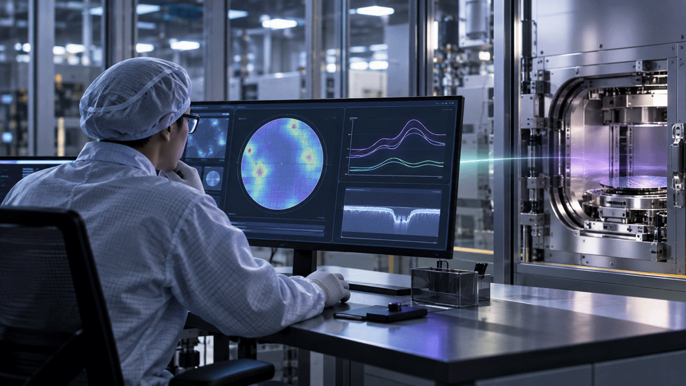

When semiconductor yield drops, the answer is usually already in the data — spread across test results, wafer histories, tool logs, and sub-fab records that no one has time to stitch together by hand. Investigating semiconductor yield loss means connecting that evidence across systems and engineering domains.
An agentic AI system does that work. It doesn’t stop at flagging that something moved: it reasons through the goal, pulls in other specialized agents, and builds what’s needed to decide the next move.
How AI Agents Investigate Semiconductor Yield Loss
The steps below trace a single yield excursion from alarm to recommendation. Each one hands its output to the next.
-
Read the wafer signature. The agent starts with the wafer data itself — parametric, sort, and WAT results — to establish which wafers moved and on which parameters.
-
Trace it back. It links those wafers to process routes, tool histories, and chamber conditions, returning the commonalities the data supports: what the affected wafers share that the unaffected ones don’t.
-
Correlate across domains. A process analysis agent evaluates active recipe data alongside sub-fab support systems to surface deviations that never tripped a limit — a dry pump drawing more current week over week, an exhaust line drifting inside its own bounds.
-
Surface what happened last time. It compares the event’s time-series signature against past excursions using similarity search and returns the matches with their resolutions — what the cause turned out to be, what was done, and whether it held.
-
Package the case. Trace charts, ranked candidates, and prior resolutions are assembled into a reviewable case for what to inspect, monitor, or hold.
-
Learn from the outcome. Once engineers close the issue, the diagnostic chain and its resolution are fed back into the knowledge base, so the next investigation of the same signature starts with this one.
This does not replace engineering judgment, and it does not close every investigation. A novel signature with weak correlation across domains still demands an experienced process integration engineer, and it should. Most excursions are not that. Most turn out to be a known failure mode on a known tool.
On a manual investigation, most of those steps sit with different people. A yield engineer reads the wafer data. An equipment engineer pulls the tool history. A facilities engineer checks the sub-fab. Someone digs up what happened the last time. Each handoff waits on the one before it, and on whoever is free. Here the chain runs end to end without the wait.
In a semiconductor yield loss investigation, what lands on the engineer’s desk is not a dashboard. It’s a documented chain: the wafers affected, the candidates ranked, the supporting traces, and what it turned out to be when this signature last appeared. The work arrives assembled, and the engineer spends their time weighing it rather than gathering it.